2025

TIE-M -Mechanical

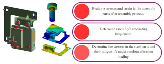
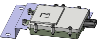
TIE M-Mechanical is a CAD Design Challenge that aims to assess students’ proficiency in computer-aided design (CAD) for mechanical components, with a focus on electronic packaging and electro-mechanical assembly as shown in Figure 1. This challenge evaluates students’ knowledge and skills acquired through coursework in mechanical engineering, emphasizing the design and manufacturing of mechanical components using CAD software. The challenge seeks to establish itself as a benchmark certification in the field of mechanical CAD design, particularly within the context of electronic packaging and electro-mechanical systems.

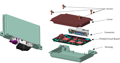
Figure 1. Electro-mechanical assembly

Objectives:

– Stimulating student’s interest in mechanical engineering and CAD design, particularly in the context of electronic packaging and electro-mechanical assembly.

– Evaluating student’s CAD design skills within a competitive framework, fostering a spirit of excellence and innovation in mechanical component design for electronic systems.

– Certifying student’s CAD proficiency endorsed by industry experts, including the Industrial -Advisory Committee (IAC), to meet industry standards and requirements for electronic packaging and electro-mechanical assembly.

– Providing the electronics industry with a pool of skilled CAD designers ready to contribute to various electro-mechanical engineering projects, including electronic packaging solutions.

– Familiarizing students with the processes involved in designing mechanical components and assemblies for electronic packaging, ensuring compatibility with electronic modules and adherence to packaging standards.

– Cultivating a high level of professionalism in the use of CAD software systems for mechanical engineering applications in the context of electronic packaging and electro-mechanical assembly.

– Increasing awareness within the mechanical engineering and electronics industries about available talent and fostering strong partnerships between academia and industry in the realm of electro-mechanical engineering.

– Generating increased demand for mechanical engineers with CAD design skills specialized in electronic packaging and electro-mechanical assembly among current students and expanding job opportunities within the industrial sector.


Description of a subject (summary)

As a mechanical design engineer, your company won a project to create a sensor module for a well know OEM car manufacturer. To boost profits and speed up development, the company chose to use existing components (Figure 2) and make design ajustments to meet the client’s needs. Modifications to the bracket and sensor ensure they fit within specified areas without altering overall functionality. The client provided a 2D drawing (“Cover.pdf”) as a starting point for the cover design, which must be optimized to meet all requirements. The 3D model includes restricted areas for the new parts.

Figure 2 Existing components


Solution

The criteria on the basis of which the student qualifies as being initiated in the evaluated topic:

– Understanding Electronic Packaging: Show knowledge of how to place electronic components and manage heat within CAD designs.

– Efficient Component Integration: Ability to seamlessly integrate electronic parts into mechanical designs while meeting industry standards.

– CAD Proficiency: Expertise in using CAD software to design, model, and simulate electronic assemblies.

– Creative Problem-Solving: Demonstrate innovative solutions to electronic packaging challenges within CAD designs.

– Detail-Oriented Design: Attention to detail in CAD designs, including precision in measurements, accurate placement of components, and consideration of assembly constraints and tolerances for electronic packaging.

– Compliance with Standards: Ensure that CAD designs meet industry standards and client requirements.

– Clear Communication: Clearly convey design intentions through CAD drawings and documentation for effective collaboration.

– Professionalism: Maintain professionalism by meeting deadlines, accepting feedback, and handling information ethically.


Alina Spânu, POLITEHNICA Bucuresti Alexandru Falk, Continental Autonomous Mobility

TIE E Committees


Chair:

Liviu VIMAN, Technical University of Cluj-Napoca

Co-Chairs:

Mihai CENUȘĂ, Continental Automotive, Iași
Mihaela PANTAZICĂ, POLITEHNICA of Bucharest


Technical Committee – Academic Trainers

Chair:

Mihaela PANTAZICĂ, POLITEHNICA of Bucharest

Co-Chairs:

Adrian PETRARIU, Ştefan cel Mare University of Suceava

Academic Members:

Alexandru AVRAM, 1 Decembrie 1918 University of Alba Iulia

Iulian BOULEANU, Lucian Blaga University of Sibiu

Iulian BUŞU, POLITEHNICA of Bucharest

Marius CARP, Transilvania University of Braşov

Mihai DĂRĂBAN, Technical University of Cluj-Napoca

Silviu EPURE, Dunărea de Jos University of Galaţi

Sanda-Diana FIRINCĂ, University of Craiova

Raul FIZEȘAN, Technical University of Cluj-Napoca

Daniela IONESCU, Gh. Asachi Technical University of Iaşi

Septimiu LICĂ, Politehnica University of Timişoara

Cristian Marius LUPOU, Politehnica University of Timişoara

Alin Gheorghiță MAZĂRE, POLITEHNICA of Bucharest, University Center of Piteşti

Mădălin MOISE, POLITEHNICA of Bucharest

Mihai NEGHINĂ, Lucian Blaga University of Sibiu

Adrian TĂUT, Technical University of Cluj-Napoca

Industrial Committee

Chair:

Mihai CENUȘĂ, Continental Automotive, Iași

Industrial Co-Chair:

Bogdan POPESCU, Microchip Technology, Bucureşti

Mugur Dobre, Founder “Cercul de electronică” / Freelancer, Munchen,
Germania

Academic Co-Chair:

Gabriel CHINDRIŞ, Technical University of Cluj-Napoca

Industrial Members:

Aurelian BOTĂU, Continental Automotive, Timişoara

Norbert BUCHMULLER, Robert BOSCH SRL

Valentin-Cătălin BURCIU, Draexlmaier Romania

Alexandru CHISER, Microchip Technology, Bucureşti

Mugur DOBRE, Founder “Cercul de electronică” / Freelancer, Munchen, Germania

Florin Alexandru DURUS, Robert BOSCH SRL

Alexandru EFROS, Continental Automotive Systems, Sibiu

Nicolae GROSS, Continental Automotive Systems, Sibiu

Alexandru KNIZEL, Continental Automotive, Timişoara

George LUCACI, Robert BOSCH SRL

Florin-Bogdan MARANCIUC, Continental Automotive Systems, Sibiu

Marian-Călin NEMEȘ, Continental Automotive Systems, Sibiu

Flaviu NISTOR, Continental Automotive Systems, Sibiu

Costin ONOFREI, Robert BOSCH SRL

Csaba TĂRCEAN, Continental Engineering Services, Timişoara

Corneliu TOMA, Digitech SRL, Bucureşti

Mihai VIDRAŞCU, Autonomous Flight Technology, Bucureşti

Radu VOINA, KEYTEK Innovation, Alba Iulia


TIEE Academic & Industrial Assesors:

Ciprian ABRAMOV, Microchip Technology

Dorin ANTONOVICI, IFM Sibiu

Iulian BOULEANU, Lucian Blaga University of Sibiu

Marius CARP, Transilvania University of Braşov

Andreea CHIOREANU, POLITEHNICA of Bucharest

Alexandru CHISER, Microchip Technology

Mihai DĂRĂBAN, Technical University of Cluj-Napoca

Alexandru EFROS, Continental, Sibiu

Cosmin Ionuț FRIMU, Miele, Brașov

Nicolae GROSS, Continental, Sibiu

Alexandru KNIZEL, Continental Automotive Timișoara

Florin-Bogdan MARANCIUC, Continental, Sibiu

Alexandru Ionuț MARIN, Miele, Brașov

Mădălin MOISE, POLITEHNICA of Bucharest

Cosmin ONCIOIU, POLITEHNICA of Bucharest

Mihai SAIN, Microchip Technology

Csaba TARCEAN, Continental Automotive Timișoara

Liviu VIMAN, Technical University of Cluj-Napoca

TIE-M Plus: Accept the Structural Challenge


Finite element analysis (FEA) is a numerical method used for predicting how an object or an assembly behaves under given physical conditions.

It is necessary to use mathematics to comprehensively understand and quantify any physical phenomena such as solid mechanics, fluid mechanics, electromagnetics, heat transfer, acoustics, or other physical effects.

Most of these phenomena are described using Partial Differential Equations (PDEs). Solving these PDEs, even by using computational methods, required the development of specific numerical techniques over the last few decades, out of which a prominent one is the FEA.

Engineers in various industries heavily rely on FEA, because of its benefits including increased accuracy of prediction, better insight into critical design parameters, virtual prototyping, fewer hardware prototypes and experimental validations, a faster and less expensive design cycle, increased productivity, and, overall, an increased revenue.

Starting from 2023, TIE introduced a new section called TIE-M+, focusing on structural and thermal management analysis of electronic packaging. The contest provides students with a comprehensive electronics development experience concerning structural integrity aspects.

Picture 1 – Example of a product chosen for the simulation contest

Organizing such a FEA competition in Romania helps to fill the gap in a multidisciplinary contest, offers an opportunity for students to relate their theoretical knowledge to practical examples, and helps to bring together specialists and experts from the industrial and academical partners.

The subjects the students must develop are focusing on different types of electronic modules, such as particular control units or sensors, coming from the forefront of the automotive industry, including business areas like Architecture and Networking or Autonomous Driving.

The goal is to have the students understand the product and its weak spots, properly design a path towards its numerical evaluation (e.g., PCB deformation, natural frequency, and mode shape analysis) and give recommendations for design optimizations to improve system performance.

The general objective of the structural simulation contest is to familiarize the students to the basic knowledge regarding numerical simulations. In addition to this, a specific objective is to familiarize the contestants to the state-of-the-art practical workflows used within industry, to prepare the future engineers for a career in the structural simulation field.

Picture 2 – Numerical model and the corresponding subjects required


Tamas Krausz, Continental Automotive Romania

Ștefan Sorohan, Politehnica Bucharest, Romania

TIE-µ: a new TIE topic launched in 2024


Welcome to the TIE-µ

Gordon Moore famously predicted in his” Moore’s Law” paper that it might become more cost-effective to construct extensive systems using smaller, individually packaged functions interconnected together. More than half a century later, the structure of the System-on-a-Chip (SoC) changes significantly with the partitioning of a monolithic die into smaller chiplets: packaging becomes one of the main focuses when designing a chip and the way the initial functionality is partitioned between multiple chiplets and how these are interconnected means we must shift our perspective to Systems in Package (SiP) (source: A. Jâjâie, A. Puşcaşu, I. Ailenei, C. B. Ciobanu and P. Svasta, “Chiplets and Next-gen Packaging Technologies in University Education,” 2023 IEEE 29th International Symposium for Design and Technology in Electronic Packaging (SIITME), Craiova, Romania, 2023, pp. 207-214, https://doi.org/10.1109/SIITME59799.2023.10431355)


As the industry shifts towards heterogeneous integrations, systems in package and chiplets it becomes of paramount importance to train future engineers in these state-of-the-art techniques, including employing interposers, 2.5D, and 3D integration.


Starting from this year, TIE introduces a new topic – TIE-μ, which is addressing important subjects such as advanced packaging, 2.5D/3D integration and chiplets. In this regard, TIE is a unique approach and to our knowledge the only one of this type in Europe which bridges the gap between Universities, Industry and advanced topics such as Chiplets as shown in Figure 1. The contest brings all stakeholders to the table, ensuring industry relevant data sets are proposed as topics using state of the art EDA tools in an academic environment, in order to introduce future engineers to an upcoming future career path in advanced packaging, chiplet integration and heterogenous design.

Figure 1 Interaction between Industry, Universities and Chiplets

As illustrated in Figure 2 (source: https://www.nature.com/articles/s41928-024-01126-y), the modern approach for heterogenous integration requires high speed interfaces such as Universal chiplet interconnect express (UCIe) and advanced packaging. TIE-μ focuses on the new interconnection challenges for high-speed interfaces, interposers and other techniques the students need to prepare for when transitioning from SoC to SiPs. SiPs make use of specialized chiplets with customer IP and memory on the same package.

     Figure 2 Heterogeneous open chiplet on-package


More information about TIE-μ

For sponsoring the event and obtain valuable networking experience, please visit TIE 2025 Partners and Sponsors.

TIE-E Plus Contest Regulation


  1. General

The present document outlines the primary factors to consider prior to and after enrollment in the TIE-E Plus competition. We would kindly ask you to read it thoroughly and for any questions you may have that are not directly addressed in the following lines you can always reach up to us at tieplus@up-see.org, and one member in the organizing committee will get back to you as soon as possible. We are dedicated to ensuring your successful participation at the event and facilitating your up-skilling process within our virtual prototyping community.

  1. Brief description

TIE-E Plus Contest is a prestigious competition established by industry professionals in collaboration with academia, with the main goal of driving froward innovative practices in engineering education, particularly focused on product virtual prototyping methods and techniques.Our objective is to help you understand current industry challenges and support you in becoming the engineer of tomorrow. We look to achieve this by exposing you to the latest technologies and industry product requirements. Thus, TIE-E Plus draws inspiration from real-life engineering challenges brought up by our industry partners and has as main goal to give you the chance to evaluate your engineering skill set against actual electronic product development challenges.

  1. Contestant profile requirements

The contestant must be enrolled at a higher education institution. Accepted profiles will fall under one of the following categories:

  • Undergraduate students
  • Graduate students
  • Master’s students
  • PhD Students

All applications will be verified by the organizing committee members. As soon as that happens you will get notified of the status of your application.Besides that, the contestant shall have a minimum idea about the contest’s scope and show at least basic skills using the tools needed to solve the proposed subject.Knowledge of English language (B1 level at least) is mandatory, as the subject presentation, trainings, and final report are/shall be written in English.

  1. Workflow

Further, a step-by-step guide for registering will be presented.

  1. First, identify the section you want to register to: Signal and Power Integrity, Thermal Management or Structural Analysis
  2. Fill in the registration form with the requested information.
  3. An acceptance or rejection notice will be sent to you.
  4. You will receive in your acceptance email the links to the specific group for your section. Please register and join the indicated group.
  5. During the solving period you’ll have access to a database of knowledge prepared by the technical committee members and a series of workshops. Feel free to join discussions and debates related to the subject.
  6. Solve the subject and create a report, considering the guidelines of each subject. Please remember that the quality of the report plays a major role in the evaluation.
  7. Upload the finished report and wait for our notification to see if you qualify to the next phase.
  8. Finalists will give a brief presentation on the 2nd of April, live, in Brașov, where they shall defend their approach, with arguments and examples, debating together with the committee.

Please be aware that the quality of your presentation plays a major role in the overall final evaluation. The preliminary results after the initial report analysis may change drastically after the final presentation.We encourage collaboration and discussions with academic coordinators or other peers, yet we do not tolerate cheating. Do not upload a solution that was not developed by you, as we will find out later, during live presentations.Good luck!

TIE M PLUS Committees

Chair:

Tamas KRAUSZ, Continental Automotive Romania

Co-Chair:

Daniel COMEAGĂ, POLITEHNICA Bucharest

Technical Committee – Academic Trainers

Chair:

Ștefan SOROHAN, POLITEHNICA Bucharest, Romania

Members:

Daniel COMEAGĂ, POLITEHNICA Bucharest

Sergiu Valentin GALANTANU, Politehnica University of Timişoara

Emil NIȚĂ, POLITEHNICA Bucharest

Ștefan SOROHAN, POLITEHNICA Bucharest, Romania

Industrial Committee

Chair:

Ionut VERZEȘ, Continental Autonomous Mobility Timișoara

Members:

Philip COANDĂ, Continental Automotive Romania

Ionuț AILINEI, Continental Automotive Romania Timișoara

Eduard-Sebastian CSUKAS, Continental Automotive Romania Timișoara

Ionuț VERZEȘ, Continental Autonomous Mobility Timișoara

Adina VATAMAN, Continental Autonomous Mobility Timișoara

Cosmin FRUNZĂ, Continental Automotive Romania Iasi

Răzvan STANCA, INAS SA

Extended technical and scientific resources for TIE-E 2025 international design contest

Download PDF

Standards

IPC CHECKLIST for Producing Rigid PCBAs;
IPC-2221 – Generic Standard on Printed Board Design;
IPC-2222 – Sectional Design Standard for Rigid Organic Printed Boards;
IPC-2223 – Sectional Design Standard for Flexible Printed Boards;
IPC-7351 – Generic Requirements for Surface Mount Design and Land Pattern Standard;
IPC-2141 – Controlled Impedance Circuit Boards and High Speed Logic Design;
IPC-2581 – Generic Requirements for Printed Board Assembly Products Manufacturing Description Data and Transfer Methodology;
IPC-4101 – Specification for Base Materials for Rigid and Multilayer Printed Boards;
IPC-6012 – Qualification and Performance Specification for Rigid PCBs;
IPC-7525 – Stencil Design Guidelines;
IPC-7527 – Requirements for Solder Paste Printing;
IPC-A-600 – Acceptability of Printed Boards.

Books

» Coombs C. F., Jr., “Printed circuits handbook” – 6th edition, McGraw Hill Professional, 1000 pp., 2007, ISBN 978-0071510790;
» Harper C. A., „Electronic packaging and interconnection handbook”, McGraw-Hill, 2000;
» Lau J., Wong C. P., Prince J. L., Nakayama W., „Electronic Packaging – Design, Materials, Process and Reliability”, McGraw-Hill, 1998;
» Johnson H., Graham M., „High-speed digital design, a handbook of black magic”, Prentice Hall PTR, New Jersey, 1993;
» Brooks D., „Signal Integrity Issues and Printed Circuit Board Design”, Prentice Hall PTR, 432 pp. 2003;
» Bogatin E., „Signal and Power Integrity – Simplified”, Prentice Hall, Boston, 2010.
» Jamnia A., „Practical Guide to the Packaging of Electronics: Thermal and Mechanical Design and Analysis”, 2nd edition, CRC Press, 2008;
» Harper C. A., „High Performance Printed Circuit Boards”, McGraw-Hill professional engineering, Professional Engineering, McGraw-Hill, 2000;
» Ulrich R. K., Brown W. D., „Advanced electronic packaging”, 2nd edition, IEEE Press – Wiley, 812 pp., 2006;
» Xingcun C. T., „Advanced Materials for Thermal Management of Electronic Packaging”, Springer Science & Business Media, 2011;
» Jin Y., Wang Z., Chen J., “Introduction to Microsystem Packaging Technology”, CRC Press, Boca Raton, 218 pp., 2011;
» Rohsenow W. M., Hartnett J. P., Cho Y. I., “Handbook of heat transfer”, McGraw-Hill, 1998;
» Ganesan S., Pecht M., “Lead-free Electronics”, John Wiley & Sons, New Jersey, 766 pp., 2006;
» Tummala R., Rymaszewski E. J., Klopfenstein A. G., „Microelectronics Packaging Handbook: Technology Drivers”, Part 1, Springer Science & Business Media, 2012.

Download TIE Contest Regulation [PDF]

TECHNOLOGIES of INTERCONNECTIONS in ELECTRONICS (TIE-E)

‑ INTERNATIONAL PROFESSIONAL STUDENT CONTEST ‑

I. PURPOSE AND OBJECTIVES

TIE-E scientific and technical student event has the main purpose of evaluating and certifying the level of students’ knowledge, skills and abilities in the field of technological computer aided design (CAE-CAD-CAM) of printed circuit boards (PCB) and electronic modules, with focus on both THT (through hole technology) and SMT (surface mount technology) technologies.
The contest is based on the knowledge obtained during the electronics courses for design and manufacturing of analogue, digital and mixed electronic modules, as well as on the advanced knowledge of developing PCB interconnection structures according to IPC (Association Connecting Electronics Industries) and other international standards recognized by the electronics industry worldwide. TIE-E event is intended to be a guild certification, a brand in the field of PCB design.

Aim of the contest:
• Arousing the students’ interest in the electronic packaging issues and PCB interconnection structures;
• Evaluating of knowledge in a competitive environment;
• Certifying by industry, with the support of the IAC (Industrial Adviser Committee), of competitors’ CAD skills;
• Supporting the electronics industry with professional human resources.

Objectives:
• Familiarizing the students with the necessary activities for designing the electronic projects of the analogue, digital and mixed modules and the PCB interconnection structures, in order to meet the demands required by the project/product specifications;
• Reaching a high level of professionalism in using CAD software systems in this field;
• Rising the awareness of the electronics industry on the existing human resources and realizing a strong partnership between academia and industry;
• Increasing job demands for the career of electronics engineer from today students and of job offers from the industrial environment.

II. ORGANIZATION

The international student contest “TECHNOLOGIES of INTERCONNECTIONS in ELECTRONICS (TIE-E)” is coordinated by the National University of Science and Technology “Politehnica” Bucharest, Centre for Technological Electronics and Interconnection Techniques. The event is yearly organised, in an itinerant way, by a university member of the EPETRUN consortium and network (Electronic Packaging Education Training and Research University Network), being also opened to all European universities interested in education and training in the field of electronic packaging.


     The contest is supervised by six committees:

a. Steering Committee (SC);

b. Technical Committee (TC);

c. Local Committee (LC);

d. Industrial Adviser Committee (IAC);

e. Public Relations Committee (PRC);

f. International Consultant Committee (ICC).

In the above mentioned committees take part representatives of EPETRUN, European universities, specialists from industry and members of non-guvernamental organizations involved in electronics. These committees take care of all technical and organisational aspects of the contest and of the whole TIE-E event.


The contest has two stages:  

  1. 1. local stage (which takes place in each university centre interested to participate toTIE-E);
  2. 2. final stage (which takes place in an university centre selected by the steering committee at least one year before the contest).


The subjects and the evaluation form will be proposed by the IAC (Industrial Adviser Committee) and will be completed/finalized by the TC (Technical Committee).

On the day before the contest day, TC will finish and optimize the subjects and the evaluation form.

On the contest day, TC + IAC will define the “evaluation teams” involved in evaluation of students (each composed of minimum two officials/experts) and the “supervisory team” (which validates the final score of the student, if necessary).

The supervisory team is activated and requested for an additional evaluation only in case of ambiguity during the evaluation process in order to decide the final score. If not necessary, the final score is set by the evaluation team.

The students will be informed regarding this important issue in the newly released TIE-E regulation and during the technical meeting which takes place on the day before the contest day.

The evaluation form will contain three signatures, two belonging to the evaluation officials/experts and one belonging to the evaluated student; if necessary, additional signatures for the supervisory team will be placed on the form.

The student will leave the contest seat/place only after the evaluation form is totally finished and closed (by the signatures specified above).


III. TOPICS *

  1. 1. CAD design of electronic circuits (SCM, SCH);
  2. 2. Creation of virtual components (parts);
  3. 3. SCM post-processing (generation of netlists, reports, export/import files, post-processing files for technical documentation);
  4. 4. CAD design of on-board interconnection structures (PCB);
  5. 5. Creation of PCB footprints;
  6. 6. Professional inter-tool communication techniques between SCM and PCB environments;
  7. 7. PCB post-processing (generation of netlists, reports, export/import files, post-processing files for technical documentation and manufacturing);
  8. 8. Standardization elements for PCB design;
  9. 9. Elements of analogue, digital and mixed design;
  10. 10. Elements of signal integrity, power integrity and electromagnetic compatibility at the PCB level.

* see on www.tie.ro all the technical topics/issues requested by TC.

IV. CONTEST RULES


  1. 1. Each university can participate at the final stage with 4 students, 3 accepted competitors and 1 reserve (student placed in the local stage ranking after the first three), possible to participate only if one of the first three students is not able to take part at the final stage due to a force majeure (an extraordinary event or circumstance beyond the control of the participating student);
  2. 2. The participation fee for a university taking part at the final stage is 200 Euro.
  3. 3. Any student can apply at the local stage of the contest if he/she proves he/she follows the courses of an accredited university;
  4. 4. The organization of the local stage is under the attributions of the universities involved in EPETRUN and other European universities;
  5. 5. The lists of qualified students for the final stage (3 + 1 reserve) will be sent by the participating university to the LC of the organising university at least two weeks before the final stage, according to the official demands;
  6. 6. The contest time for the local stage depends on local rules of the organizing university. For the final stage, the contest time is 240 minutes;
  7. 7. It will be mandatory for each student/competitor to participate with all the necessary hardware & software resources, in order to take part at the contest; the student/university has to prove the existence of the license for the CAD system used in the contest. The organizers will not provide any licensed software to the competitors, their main task being to manage the TIE-E contest and the whole scientific event around it;
  8. 8. During the contest, the student can use her/his own documentation, paper-based or in electronic format. The draft papers will be provided by LC/TC officials;
  9. 9. During the final stage of the contest, Internet access is prohibited except for CAD tool licensing purposes. Participants may bring technical documentation and consult it offline, either in digital or physical formats.
  10. 10. The contest regulations can be presented to participants at the beginning of the contest, if required;
  11. 11. During the contest, the students are not allowed to discuss things with each other, to ask explanations from another competitor regarding contest issues, to borrow personal objects or documents. During the contest, the explanations can be asked only from TC officials;
  12. 12. The contest will have an official fixed “pre-time” of 30 minutes, in which the competitors will study deeply the subjects and will ask questions; after handing-in the subjects, the students will use these 30 minutes to study the contest subjects without making any design activity on the computer and/or writing down notes and calculus;
  13. 13. The contest will have an official fixed “post-time” of 15 minutes, in which the competitors will save, archive, copy to official TC pen-drives, close applications, etc.;
  14. 14. In case of any technical problem, the student has to announce as soon as possible the situation to LC/TC officials who are supervisors in the contest room;
  15. 15. The students could benefit by the extension of the contest design time in certain conditions: hardware/software problems, breakdown of the workstation and related issues. Any other situations will not be accepted for the extension of the official contest time;
  16. 16. The evaluation at the local stage is done by one or two officials, together with the student who solved the subject. If the student is not present when the evaluation activity starts, he/she will be called when the evaluation session of his/her group ends. If he/she is still not present, his/her subject will be evaluated in his/her absence;
  17.  17. The evaluation at the final stage (see also the “II. ORGANIZATION” paragraph) is mandatory done by officials from TC and IAC, together with the student who has solved the subject. If the student is not present when the evaluation activity starts, he/she will be called later or at the end of the evaluation session. If he/she is still not present, the subject will be evaluated in his/her absence, but in the presence of a witness student from the same university;
  18. 18. The evaluation of the subjects at the final stage is public;
  19. 19. The students who participate at the final stage will be awarded with diplomas and prizes: three prizes and up to five mentions;
  20. 20. Additionally, IAC will attest the best ranked students with “PCB Designer” certificates recognized by the electronics industry;
  21. 21. The first prize winner is not allowed to participate at the future editions of the TIE-E contest;
  22. 22. The students who are not present at the contest and who are on the contest list will be referred to as “not present”, and those who leave before the contest time expires will be referred to as “abandon”;
  23. 23. The contest regulation can be found on the web-page of the contest (www.tie.ro), in English, on the web-pages of the EPETRUN university network and other participating universities, depending on the specific of their web-pages;
  24. 24. Any change in this document will be announced to all universities participating at the TIE-E contest immediately after the new version will be released.

Rev: February 22, 2024

TIE-E A story since 1992

A WAY to turn your HOBBY into PROFESSION


Welcome to the TIE-E Event!

The TECHNOLOGIES of INTERCONNECTIONS in ELECTRONICS (TIE-E) contest is a student professional contest whose objective is to promote technological computer aided design (CAE-CAD-CAM) of electronic modules. This contest brings together students from different Universities since 1992. Students have a great opportunity by taking part in this contest. A good organization and a total transparency during the contest are the main coordinates proving professionalism and fair-play among students keen on electronic packaging.


Mission

Every year TIE-E gathers the greatest student PCB designers form around the country in the ultimate showdown in which not only pride and glory are at stake, but also important prizes to be won. At the end of the contest, there can be only one winner, however, all contestants meeting a score margin established by the Industrial Advisor Committee receive a “Certificate of Competence”, recognizing their professional abilities as PCB designers.

Being in close relations with the industry, TIE-E contestants are widely sought by highly appraised companies for internships and hiring after graduating their studies. As a result, many examples of past TIE-E contestant can be found in high ranking functions at important companies around the country and around the world, often returning to TIE-E as part of the “Industrial Advisor Committee”.

TIE-E not only aims to bring industry and university together, in a tighter, more constant collaboration but under its slogan, „Turn your hobby into a profession!”, also targets to challenge students to think outside of the box, to face them with real-life design challenges and present to them what are the industry’s expectations from an engineering graduate. Therefore, besides the student contest, workshops and presentations held by both foreign universities as well as electronics companies go along with the contest every year.

Sponsors of the contest also get a chance to present their offers and products both to students and committee members, either by exposing roll-ups, banners or even presentation stands or by means of oral presentations. TIE-E welcomes everyone interested in the field of electronics, PCB design but not only to actively participate in the sponsoring and organizing the contest.

New in 2014 is the support offered by the AFCEA (Armed Forces Communications and Electronics Association), Chapter Bucharest, through AFCEA Support Committee. AFCEA Student Chapters from around the country play an important role in preparing and recruiting students for the contest, and their involvement in the contest is a vital part.

We look forward to seeing all the contestants, their advisors and committee members, as well as all our sponsors and key people who annually ensure the growth of the contest not only in its size, but also in its general acknowledgement by the industry.

For more information regarding the contest regulation, please visit TIE  Regulations, or find us on Facebook as TIE.Romania!

For sponsoring the event and obtain valuable networking experience, please visit TIE 2025 Partners and Sponsors.


Download the presentation “What Design Tool to use for TIE Contest” [PDF]