TIE-µ: third edition of industry-wide student challenge
Shaping the next generation of professional SiP designers
Gordon Moore famously predicted in his” Moore’s Law” paper that it might become more cost-effective to construct extensive systems using smaller, individually packaged functions interconnected together. More than half a century later, the structure of the System-on-a-Chip (SoC) changes significantly with the partitioning of a monolithic die into smaller chiplets: packaging becomes one of the main focuses when designing a chip and the way the initial functionality is partitioned between multiple chiplets and how these are interconnected means we must shift our perspective to Systems in Package (SiP) (source: A. Jâjâie, A. Puşcaşu, I. Ailenei, C. B. Ciobanu and P. Svasta, “Chiplets and Next-gen Packaging Technologies in University Education,” 2023 IEEE 29th International Symposium for Design and Technology in Electronic Packaging (SIITME), Craiova, Romania, 2023, pp. 207-214, https://doi.org/10.1109/SIITME59799.2023.10431355)
As the industry shifts towards heterogeneous integrations, systems in package and chiplets it becomes of paramount importance to train future engineers in these state-of-the-art techniques, including employing interposers, 2.5D, and 3D integration.
Starting in 2024, TIE introduced a new topic – TIEμ (C. Ciobanu, D. Manolescu, R. Vlăduţă, L. Chiţu, C. Moisă, M. Manofu and P. Svasta, “TIE Micro – Chiplets and Next-gen Packaging,” 2024 IEEE 30th International Symposium for Design and Technology in Electronic Packaging (SIITME), Sibiu, Romania, 2024, pp. 504-511, https://doi.org/10.1109/SIITME63973.2024.10814902), which is addressing important subjects such as advanced packaging, 2.5D/3D integration and chiplets. In this regard, TIE is a unique approach and to our knowledge the only one of this type in Europe which bridges the gap between Universities, Industry and advanced topics such as Chiplets as shown in Figure 1. The contest brings all stakeholders to the table, ensuring industry relevant data sets are proposed as topics using state of the art EDA tools in an academic environment, in order to introduce future engineers to an upcoming future career path in advanced packaging, chiplet integration and heterogenous design.
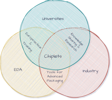
Figure 1 Interaction between Industry, Universities and Chiplets
As illustrated in Figure 2 (source: https://www.nature.com/articles/s41928-024-01126-y), the modern approach for heterogenous integration requires high speed interfaces such as Universal chiplet interconnect express (UCIe) and advanced packaging. TIEμ focuses on the new interconnection challenges for high-speed interfaces, interposers and other techniques the students need to prepare for when transitioning from SoC to SiPs. SiPs make use of specialized chiplets with customer IP and memory on the same package.
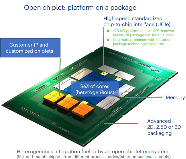
Figure 2 Heterogeneous open chiplet on-package
The main topics necessary for designing advanced packaging and interconnects include insight in layout design (package or PCB), signal and power integrity, system in package (SiP) fundamentals, timing and high frequency analysis.
For sponsoring the event and obtain valuable networking experience, please visit TIE 2026 Partners and Sponsors.