TIEn (nano)- the newcomer at the TIE Platform
-international education platform for students and talents in electronic packaging-
Today, the European Union is facing a severe shortage of skilled talent required to support the EU Chips Act. The Important Project of Common European Interest (IPCEI) provides an excellent framework to enhance and foster the development of the semiconductor industry in the EU, helping to meet the growing demand for trained engineers in this field.
At the national level, the Romanian Government has undertaken initiatives to financially support these projects, aiming to transform the country into a relevant player in the microelectronics sector. Although the semiconductor value chain cannot be fully internalized, segments such as design, physical implementation (layout), testing, and circuit validation can be successfully executed within Romania.
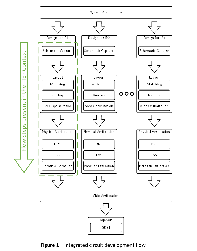
Developing these activities requires close collaboration between engineering universities and the industrial sector to equip future engineers with up-to-date and relevant skills. Figure 1 presents a reduced set of activities involved in the integrated circuit development process, illustrating the flow required to develop a functional module for chip integration.
For years, the Technologies of Interconnection in Electronics (TIE) platform has connected Romanian universities with the electronics industry to cultivate specialized talent. Building on this legacy, extending the competition to include TIE-n (nano) is a strategic step. By combining micro- and nano-technologies, TIE provides a robust ecosystem for assessing student knowledge, ranging from integrated circuits and System-in-Package (SiP) technologies to complex PCB design. Beyond education, TIE serves as an industryrecognized challenge, certifying that students possess the electrical, mechanical, and thermal design skills demanded by the market.
Within the framework of the TIEn challenge, the process begins with Schematic Capture based on established standards, using PDK components and documenting critical layout constraints such as electromigration requirements, device matching, and noise sensitive nodes. Once validated, the schematic is transitioned to the layout phase, where the designer implements decisions regarding device matching (e.g., common centroid), optimal routing (including shielding and star connections), and floor planning. Following the initial layout iteration, the design undergoes three standard Physical Verification steps, i) DRC (Design Rule Check), ii) LVS (Layout vs. Schematic), and iii) PEX (Parasitic Extraction), which are essential for evaluating the implementation quality. Once the physical design passes all checks and meets the required specifications, it is integrated into the full chip for final verification and GDSII file generation for fabrication.
The transition to deep-submicron technological nodes introduces major complexities in the physical implementation stage. Design efforts face obstacles generated by manufacturing process limitations (such as WPE, STI stress, and matching issues), the influence of parasitic elements (RC), and thermal constraints caused by increased power density. Since these phenomena directly degrade circuit performance, the responsibility for mitigating them falls predominantly on the physical design and layout implementation stage.
This rigor in physical implementation becomes even more critical in the era of chiplet technologies, a strategic direction supported by the Romanian Government through funding instruments such as IPCEI ME/CT and POCIDIF. Layout activity for IP blocks forms the foundation for generating chips that are subsequently integrated into these advanced heterogeneous systems, which are essential for artificial intelligence and data processing. Thus, physical design competencies contribute directly to consolidating a competitive national ecosystem that unites universities, research centers, and industrial partners.
Starting in 2026, the TIE family of contests takes a significant step toward cultivating integrated circuit development skills by launching the TIEn (nano) section. This section is dedicated to physical design (layout) for analog and mixed-signal circuits. The objective will be achieved by organizing a national student competition that involves implementing an analog module according to industry standards. The results will be validated by a committee composed of experts from both the private sector and academia, possessing extensive experience in the field. Thus, closing the gap between two major contributors for developing reliable electronic products, the IC designers and the product engineers.